Degrees of Separation: The Physics of Heat That No Chip Designer Can Outrun
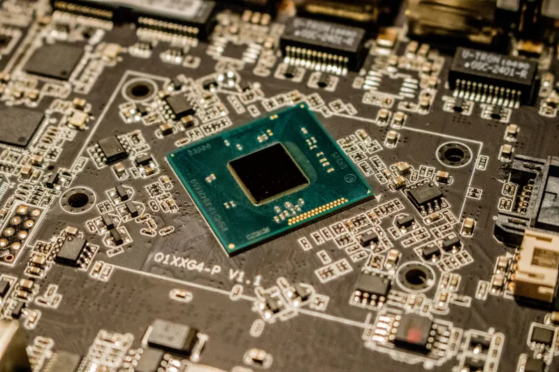
Gordon Moore's 1965 observation about transistor density was never intended as a physical law. It was an empirical trend, a pattern noticed in early data and extrapolated with engineering optimism. For roughly five decades, the semiconductor industry honored it through extraordinary ingenuity—shrinking feature sizes, redesigning architectures, and discovering new materials at a pace that made the observation feel more like prophecy than projection.
What Moore's Law never addressed, because the problem was not yet urgent when he wrote it, was heat.
At the transistor counts now standard in leading-edge processors—Apple's M-series chips exceed 100 billion transistors; NVIDIA's H100 GPU surpasses 80 billion—the thermal consequences of switching activity have become the dominant constraint in chip design. Not the lithography. Not the interconnect resistance. Not even the economics of advanced fabrication, though that constraint is severe in its own right. The hard ceiling, the one that no process node shrink can simply dissolve, is the inability to extract heat from a piece of silicon faster than physics permits.
The Thermodynamics of Thinking
Every transistor switch—the binary event of current flowing or not flowing through a microscopic gate—dissipates energy as heat. At low transistor counts, this is trivially manageable. At the densities now achievable through TSMC's 3-nanometer process or Intel's Intel 18A node, the aggregate thermal output of a chip running at full utilization can reach power densities comparable to a rocket nozzle per unit area. This is not a figure of speech. Researchers at MIT and Stanford have published power density measurements for advanced processors that approach or exceed 1,000 watts per square centimeter in localized hot spots—a figure that exceeds the surface temperature of a nuclear reactor's fuel rod in terms of heat flux.
The conventional cooling solution—a metal heat spreader, thermal interface material, a heatsink, and a fan—functions by conducting heat away from the chip surface and dissipating it into the surrounding air. This approach works adequately when power densities are moderate and heat sources are distributed. It begins to fail when power is concentrated in a small die area, when chips are stacked vertically in three-dimensional configurations, and when the thermal interface materials between layers introduce resistance that compounds with every additional tier.
The fundamental constraint is Fourier's Law of heat conduction, which describes the rate at which heat can flow through a material as a function of that material's thermal conductivity, the temperature gradient across it, and the cross-sectional area available for heat flow. Shrinking a chip increases power density while simultaneously reducing the surface area available for heat extraction. The math does not resolve favorably.
The Architecture of Compromise
The semiconductor industry's response to the thermal wall has been, characteristically, to redefine the problem rather than solve it directly. If a single large chip running at high frequency generates unmanageable heat, the alternative is to distribute computation across multiple smaller chiplets, connected by high-bandwidth interconnects, each operating at lower power densities. AMD's chiplet strategy, which disaggregated its processor designs into separate compute, I/O, and cache dies, was driven substantially by thermal and yield considerations as much as by architectural preference.
Three-dimensional stacking—placing memory or compute dies directly atop one another, connected by through-silicon vias—offers dramatic improvements in bandwidth and latency but introduces a thermal problem of its own. The bottom die in a stack receives heat from every layer above it while having the least direct access to cooling infrastructure. Engineers describe this as the "buried die" problem: the component generating the most heat may be the one farthest from any cooling surface.
Intel's Foveros packaging technology and AMD's 3D V-Cache architecture both incorporate design mitigations for this problem, including selective placement of lower-power memory dies atop higher-power compute dies to manage the heat stack. These are engineering accommodations, not solutions. The physics does not change; only the arrangement of its consequences does.
Exotic Interventions at the Research Frontier
In semiconductor research laboratories, the thermal problem is prompting investigations into cooling methods that would have seemed extravagant a decade ago.
Microfluidic cooling—in which liquid coolant is circulated through channels etched directly into the silicon substrate, microns from the transistors generating heat—has moved from academic curiosity to active development at IBM, Intel, and several DARPA-funded research programs. The appeal is straightforward: liquid cooling is dramatically more efficient than air cooling, and placing the coolant channels inside the chip eliminates the thermal resistance of the heat spreader and interface materials entirely. The engineering challenges are considerable. Fabricating microfluidic channels at chip scale, ensuring leak-proof integration with packaging, and managing the fluid dynamics at microscale all represent unsolved problems at production volumes.
Two-phase cooling, in which a refrigerant absorbs heat by changing from liquid to vapor within the cooling loop, offers even higher heat transfer coefficients than single-phase liquid cooling. Data center operators including Google and Microsoft have experimented with immersion cooling—submerging entire server boards in dielectric fluid—as a system-level thermal management strategy. For individual chips, integrating two-phase cooling at the package level remains an area of active research rather than commercial deployment.
Diamond, which has a thermal conductivity roughly five times that of copper, has attracted interest as a heat spreader material for the most thermally constrained applications. Synthetic diamond substrates have appeared in some military and specialized commercial applications. At the cost and scale required for consumer or data center processors, diamond remains impractical—though several research groups are investigating chemical vapor deposition techniques that might eventually change that calculus.
The Human Cost of the Nanometer Race
Behind the physics abstractions, the thermal wall imposes concrete costs on the people designing and building these systems. Chip architects describe an increasing fraction of their design effort devoted not to adding capability but to managing thermal envelopes—clock throttling, power gating, dynamic voltage and frequency scaling, and the complex firmware logic required to prevent a processor from damaging itself under sustained load.
The performance numbers that appear in press releases increasingly reflect burst capabilities achievable only for seconds before thermal limits force a reduction in operating frequency. Sustained performance—the figure that matters for workloads running over hours or days in a data center—is often substantially lower. The gap between peak and sustained performance has grown wider with each process generation, a trend that benchmark methodologies have been slow to reflect.
For the engineers at TSMC, Samsung, and Intel working at the boundary of what lithography and materials science permit, the thermal wall is not an abstract concern. It is the organizing constraint around which every other design decision orbits. The next generation of processors will be faster, more capable, and more efficient than the current generation. They will also be hotter, harder to cool, and closer to a physical boundary that no amount of engineering ingenuity has yet found a way to move.
The experiment continues. The thermometer keeps rising.